Hochschule Kempten      
Fakultät Elektrotechnik      
Interface Electronics       Fachgebiet Elektronik, Prof. Vollrath      

Interface Electronics


Laboratory 04: 8-bit R2R DAC (11.12.2019)

Group D ***877, ***953


OVERVIEW


Motivation


8-R2R DAC LTspice Simulation

8-bit DAC Measurment


  • OPEN LTSPICE
  • Design 8-bit DAC circuit
  • Provide value for and Voltage source
  • Simulate with DAC
  • Generate the Ramp signal Waveform


  • Settling Time

  • Digital Pattern Generation,run and see Oscilloscope
  • Explore the electrical level and here frequency specified
  • Here Rising Time for full range and Falling Time calculated
  • for 8 bit 3.3 v , level= 256, Step size = 33/256 = 15 mv
  • Triggered the settling time
  • Now for Falling time Put offset= 0 and see Final value


  • Settling Time Mid level

  • At MSB remove Upper bits for 8 bits set 1-127
  • Choose push bull ,Scale Mannual, schow 2000 sec/div
  • Edit Parameter here like Frequency , Degree here we have mit level
  • Now see the Oscilloscope we can get mit level Settling Time
  • We can also see Total Enery which is Pick to pick
  • Measuring Sine Signal & Doing FFT


    LTSPICE INL, DNL FFT Analysis


  • On Digital Pttern Generator to have sign signal there should be Binary Counter changed where use custom and edit parameter
  • Output pp and import interface file which is in text edit file. and from Oscilloscope now can see the sine wave
  • now read osci.html here export the data and will get nice curve.here map to Positive integerm,copy all values to get fft
  • Open Link FFT Tool and give data to generate Charts.
  • Here we can see INL, DNL, SNL and their values and also can calculate First Harmonics


  • Sine Measurment of Digital Calibrated 8-bit R2R DAC

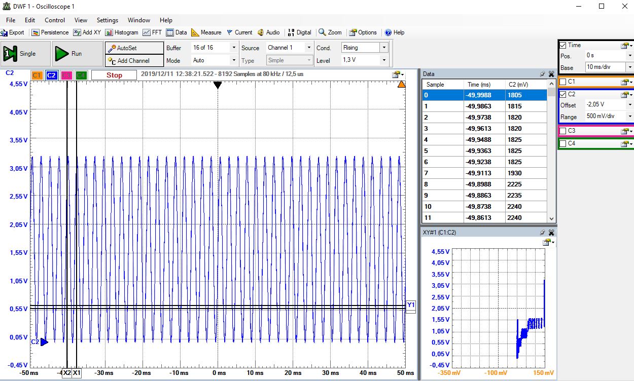
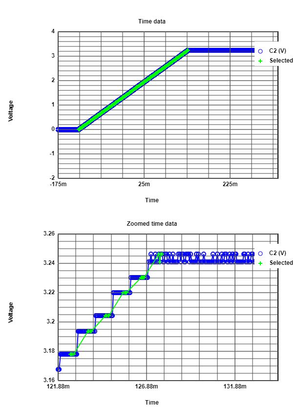
    Generate a calibration lookup table with ramp measurement


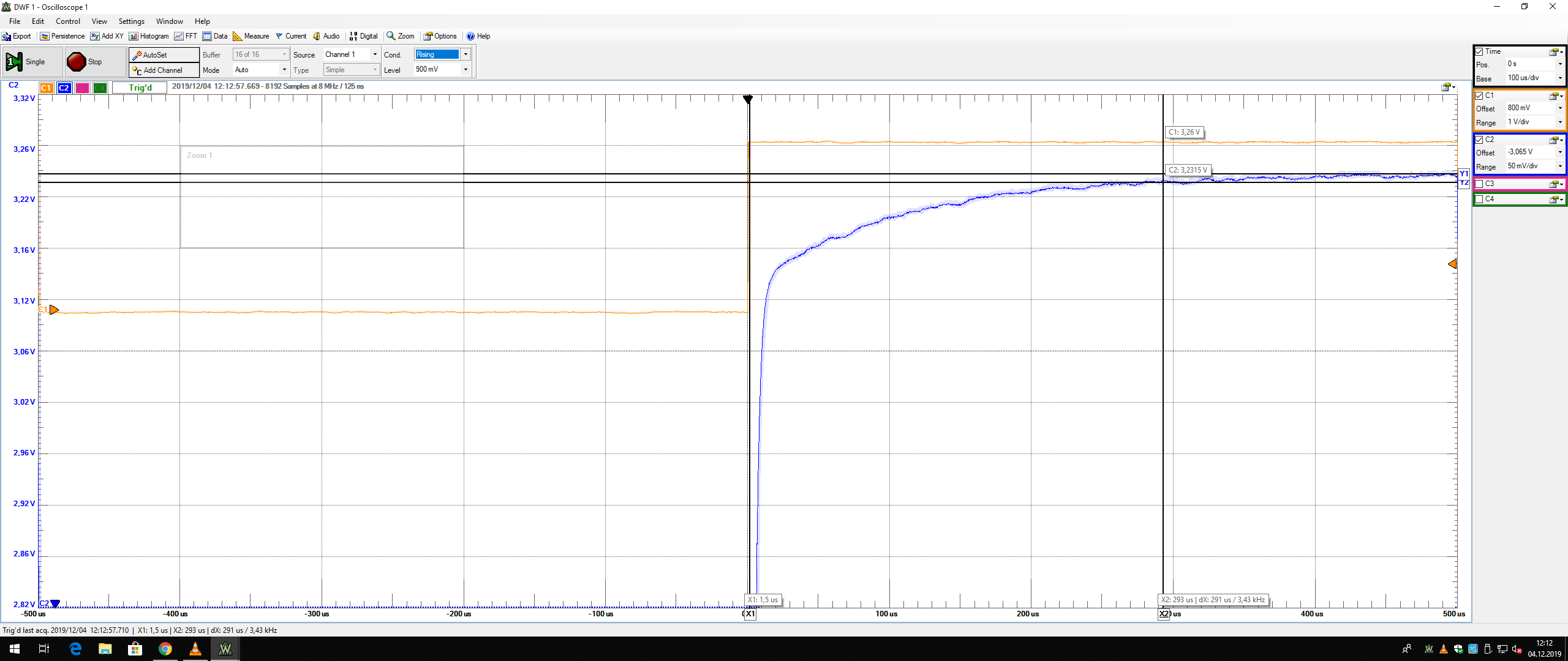
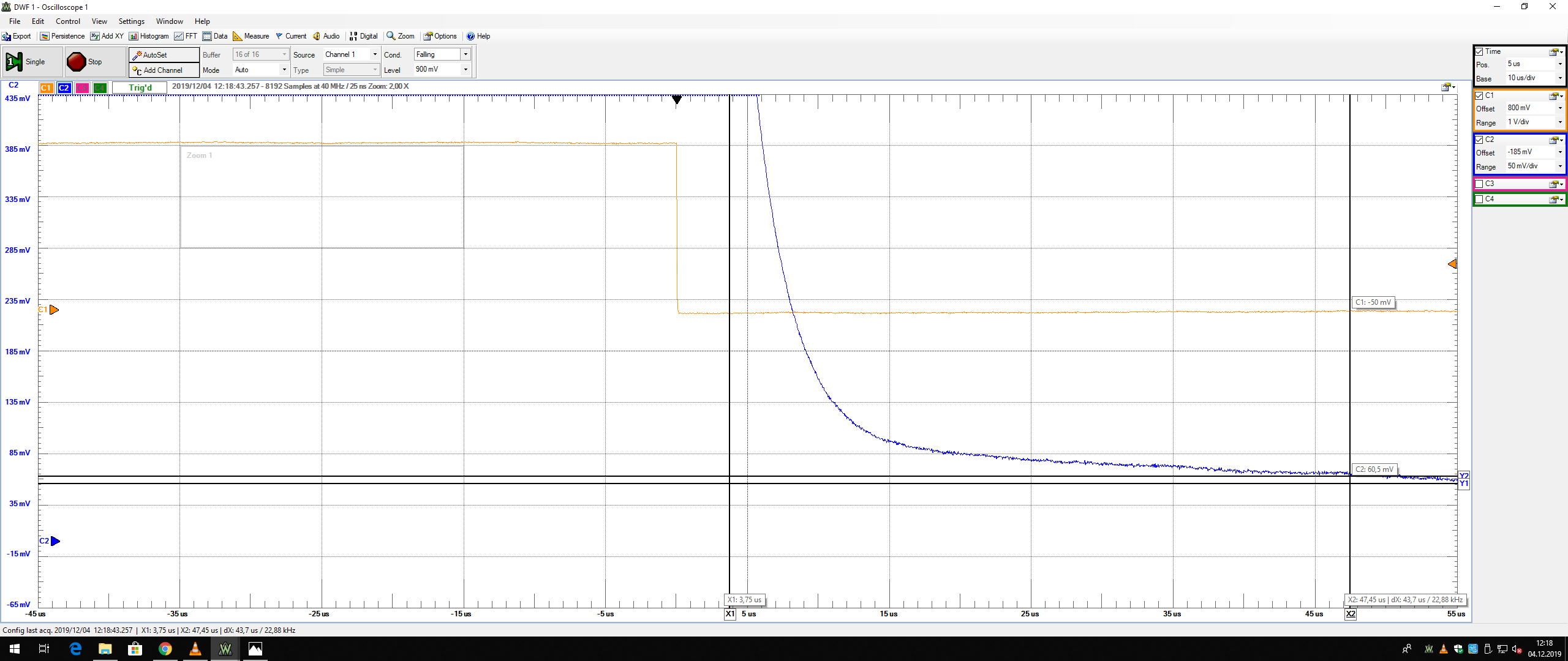
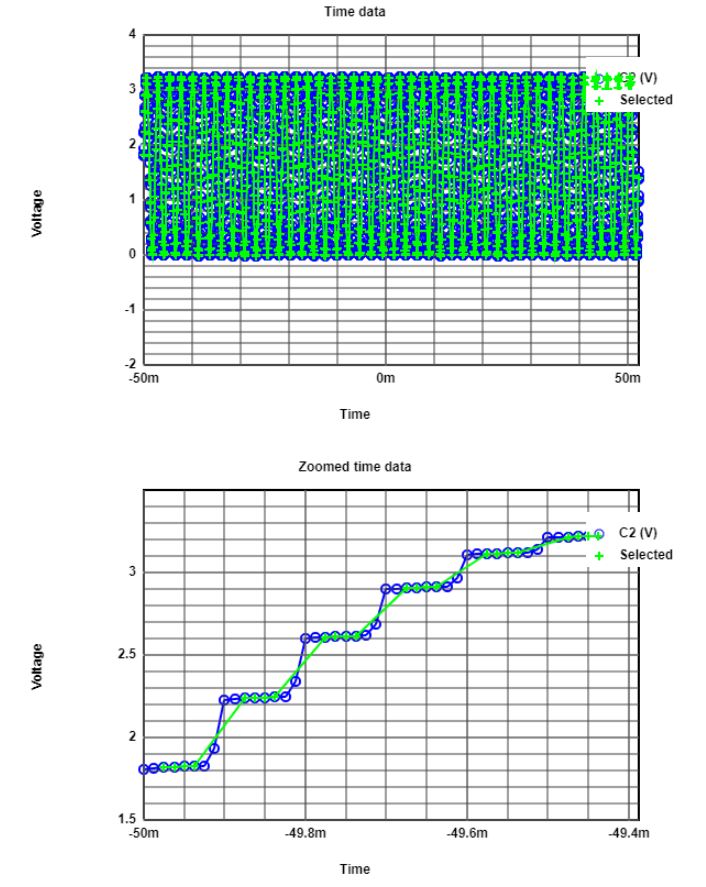
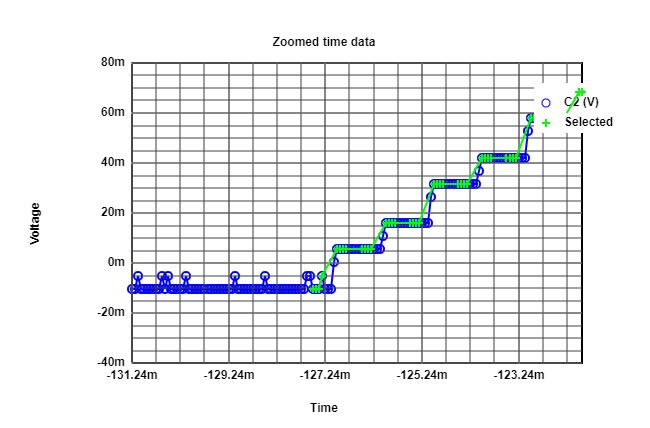
  • Here From previous wave form there are increasing and decreasing wave patterns
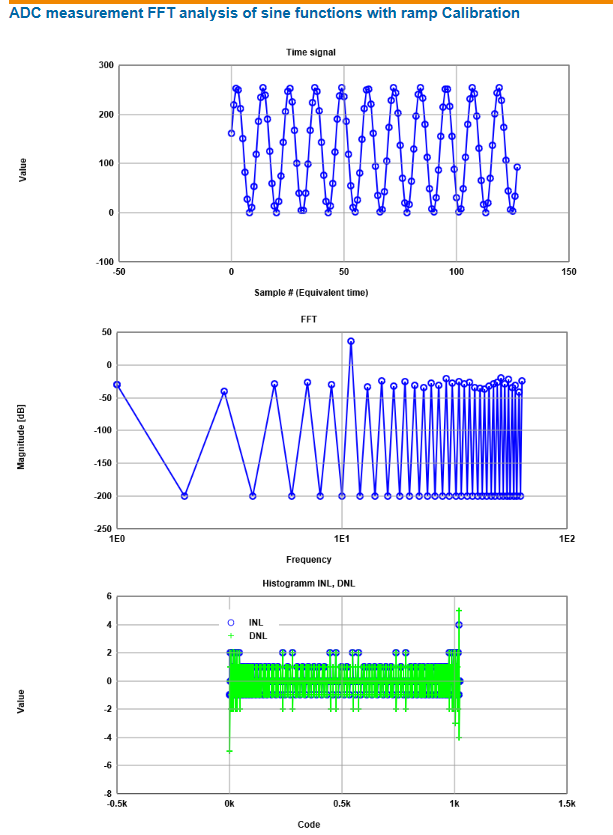
  • And also Limit Bandwidth Distortion and Settlint Time issues
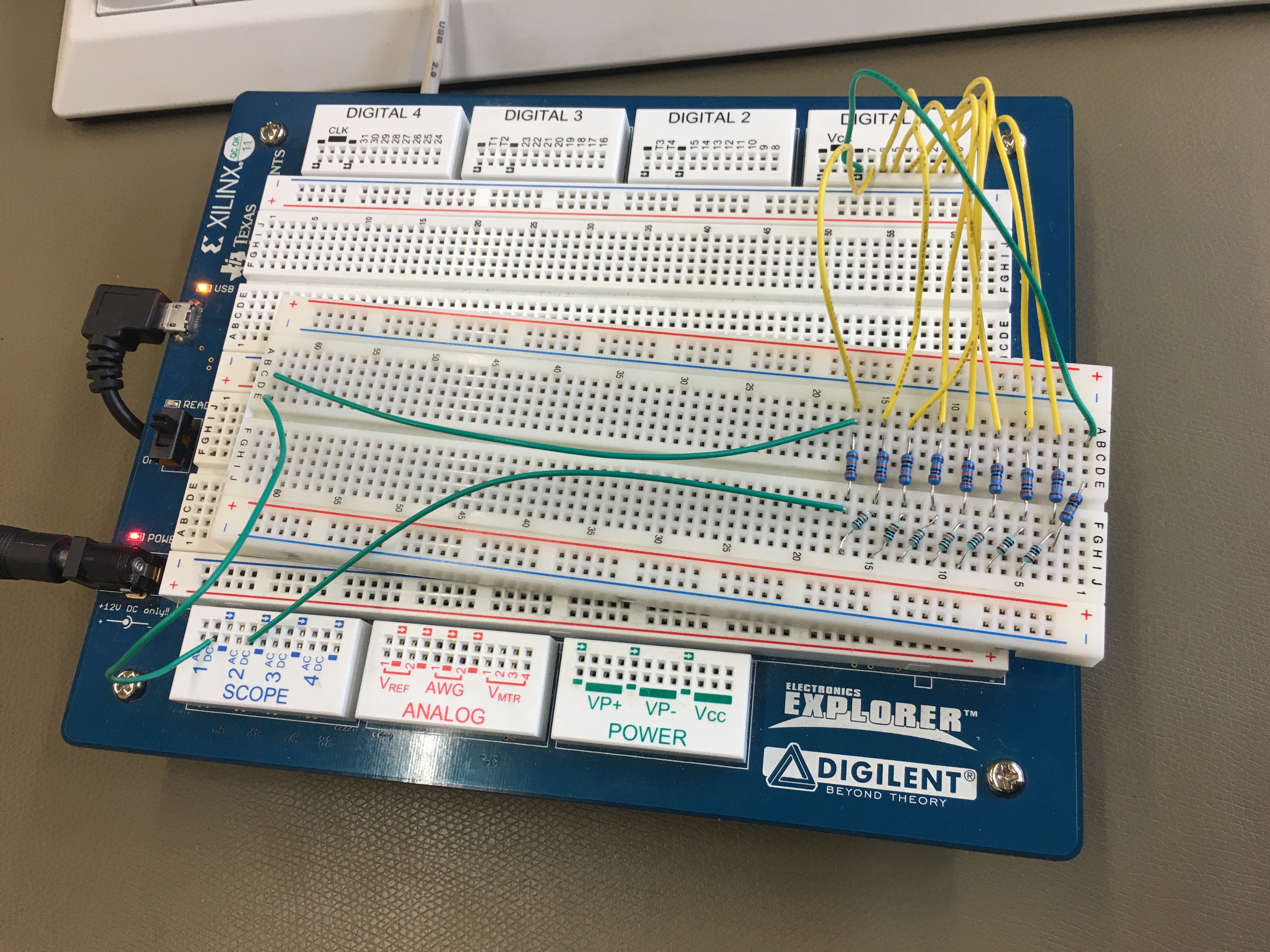
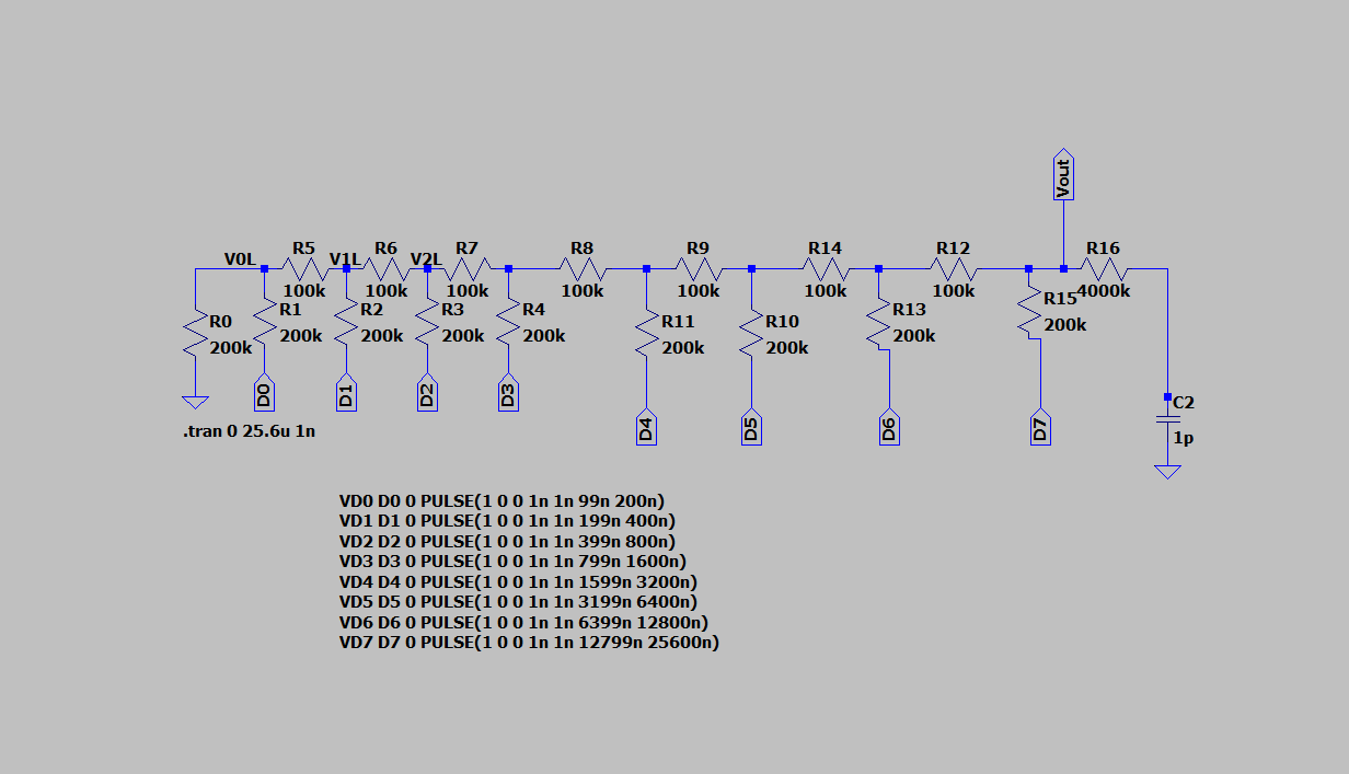
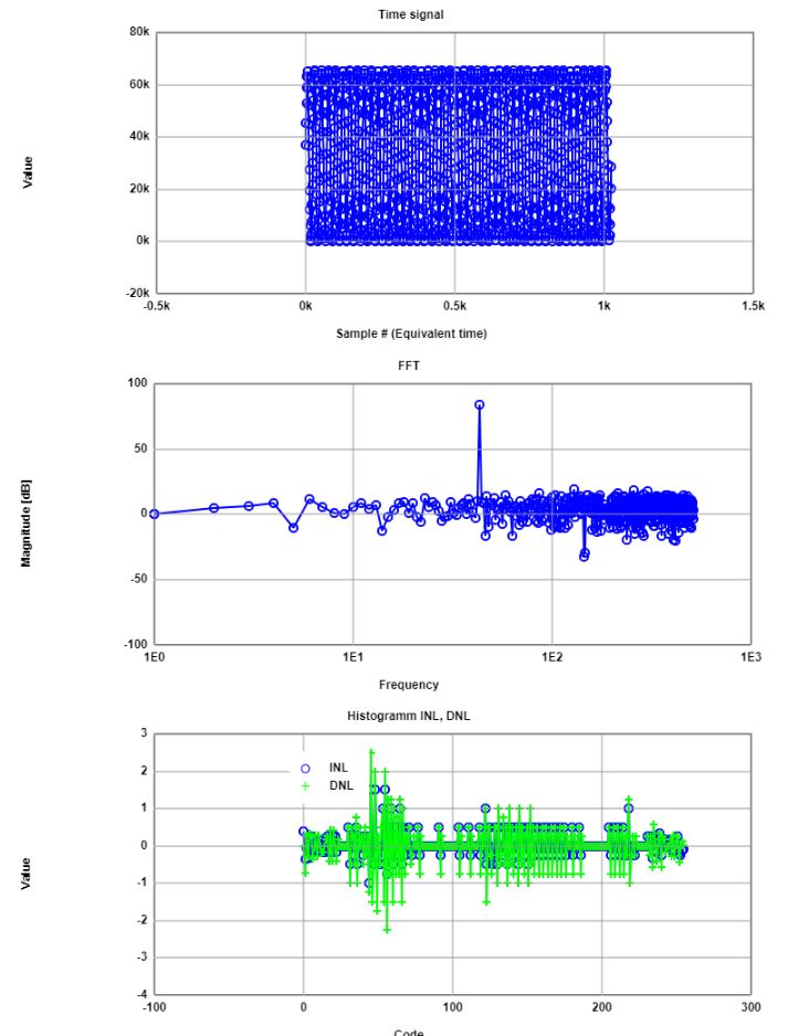
  • Now Use Read osci.html here 8 bit file imported which is Binary weighted Dac copy and check with previous.
  • Generate a new calibrated sine pattern and Measure INL, DNL and FFT with calibrated sine pattern


  • Here option where Interger values coppied & put in the DDS sim javascript_2016 html, now we use EE vector with Calibration

  • copy all data from control file of vector save it into edit file and now update the Oscilloscope
  • Export the Oscilloscope copy oscilloscope data and Replace old one o new one
  • Here we Can see Calibration improves the INL, DNL levels
  • Again sine EE vector copy text1 copy data map to Positive integer from lab sheet
  • input data in FFT_Javascript_2017_Calibration.html to generate Chart
  • Here we found that from calibrated and non Calibrated data there is 1 db difference
  • By Decreasing Number of bits we can degrease 1 bit.


  • CONCLUSION


  • Physically 8 bit DAC circuit joined on Breadboard and measured the Starting resistors values
  • During this lab, 8 bit-DAC was simulated and The simulated data was read, extracted and analysed using a provided JavaScript tool (Read Raw File).
  • A data converter with a real R2R DAC was also simulated with given data steps. Also, the simulated data was read, extracted, filtered and analysed.
  • R2R DAC is read and extracted including a sine and a ramp waveforms.
  • Correct values of resistors in the real R2R DAC were simulated. In addition to wrong values for the comparative purpuses.
  • Measured the Sign signal and FFT analysis using Link fft tool
  • Using a html webpage to publish the laboratory´s report was successfully achieved.